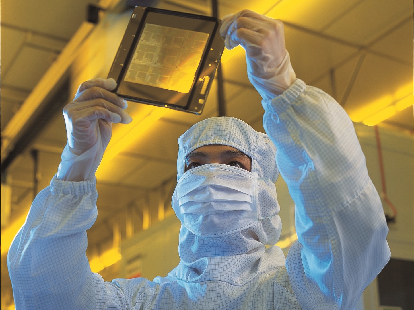
TSMC, or Taiwanese Semiconductor Manufacturing Company, is the largest semiconductor contract fab in the world building chips for some of the most well known clients such as Apple, Nvidia, and many others. Last year TSMC launched their 16nm FinFET process which is now being utilized by some of the most advanced products in the world such as the Apple A10 Fusion SoC in the iPhone 7 Plus and the Nvidia GP102 GPU in the Titan X.
Of course, TSMC isn’t stopping there as TSMC Co-CEO Mark Liu had some interesting things to say at a recent tech event in Hsinchu, Taiwan.
According to Liu, TSMC will soon be starting risk production of their 7nm process in early 2017 and is already actively in development of 5nm process technology as well. Furthermore, TSMC is also in development of 3nm process technology with 300-400 engineers already assigned to R&D. While 3nm process technology already seems so far away, TSMC is further looking to collaborate with academics to begin developing 2nm process technology.
Liu believes that for TSMC, “Moore’s Law will continue to be relevant.”
Source: DigiTimes


One nano or even smaller bit manufacturing day has arrived surely now to enable all industrial sectors speedily to realize their long-sought exponentially enhanced productivity throughout the world.