At the International Solid State Circuit Conference (ISSCC), both TSMC and Samsung had working chips samples built on their respective 7nm nodes. However, the two companies gave very different outlooks on their readiness.
According to the presentation offered by TSMC, they described the condition of their 7nm node as “healthy”. Samsung on the other hand, had a bit less confidence in its production method, showcasing a development chip that suggests 7nm chips may not be ready for at least a few more years.
The reason behind the contradicting prospects is due to the different manufacturing techniques. Because TSMC will likely be producing the Apple A11 SoC based on its 10nm node, it has to opt for the more mature High-Potassium Metal Gate (HKMG) design to ensure the chip’s workability. Samsung, on the other hand, doesn’t have this demand to meet. Though one could say that it’s losing out on a bulk of the business, this gives the Samsung some time to perfect Extreme Ultra-Violet Lithography techniques that will help improve the performance of its 7nm chips and will be instrumental going beyond 7nm as well.
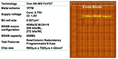
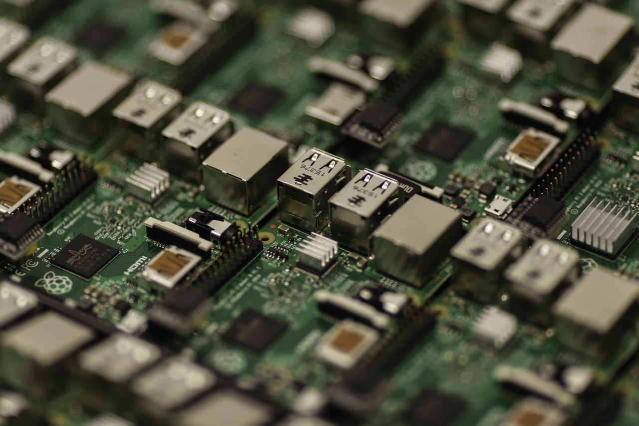
During the conference, TSMC presented a 256Mb SRAM test chip using its 7nm technology. Jonathan Chang, director of TSMC’s memory group, believes that this is the smallest SRAM to be in risk production this year. Each SRAM cell block covers an area of 0.027μm², which is just 34% the area of its 16nm counterpart. Expected chip area is 42mm².
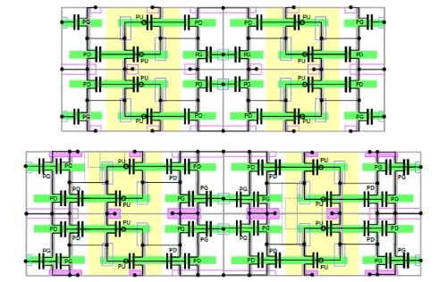
Samsung on the other hand also had a chip to show, but its product was limited to just 8Mb. As shown above, Samsung’s 7nm SRAM chip will be 30% smaller than its 10nm SRAM chip. The chip however, wasn’t made using a production ready technique, but instead built using an EUV repair process. As such, it doesn’t speak a whole lot about how far along Samsung is with EUV development.
EUV is expected to be first widely deployed beginning in 2020.
Source: EETimes


