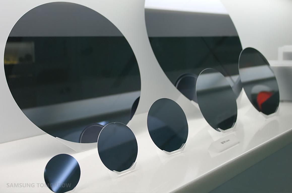
Samsung recently held the Samsung Foundry Forum event at their Device Solutions America headquarters and made some big announcements for their foundry customers.
Among the new announcements is the introduction of Samsung’s 14LPU 4th Generation 14nm FinFET process. 14LPU builds on their 3rd Generation 14LPC process, delivering additional performance at the same power and design rules of 14LPC. According to Samsung, 14LPU will be aimed at high performance and compute intensive applications.
Although Samsung just began mass production of products based on their 10nm FinFET process last month, they also announced their 3rd Generation 10LPU 10nm FinFET process. According to Samsung, 10nm LPUis expected to be the most cost effective, cutting edge process technology on the market. 10LPU will be offered with Samsung’s high performance 10LPP 2nd Generation 10nm FinFET process to cover all applications that can benefit from the 10nm process.
“After we announced the industry’s first 10nm mass production in mid-October, we have now also expanded our lineup with new foundry offerings, 14LPU and 10LPU,” said Ben Suh, Senior Vice President of foundry marketing at Samsung Electronics. “Samsung is very confident with our technology definitions that provide design advantages on an aggressive process with manufacturability considerations. We have received tremendous positive market feedback and are looking forward to expanding our leadership in the advanced process technology space.”
In addition, Samsung also showcased their 7nm EUV wafer and updated their 7nm EUV development status. No word on when development of 7nm EUV process technology will be complete at this time.
Samsung will begin offering 14LPU and 10LPU process design kits in 2Q2017.
Source: Samsung