Samsung and SK Hynix had a lot to show off in the previous weeks with back to back to back Flash Memory Summit followed by Intel Developer’s Conference and now Hot Chips.
At the HotChips conference, Samsung already talked about what to expect with GDDR6, and both Samsung and SK Hynix also talked about their work on HBM3 (or xHBM, Extreme HBM, HBMx, and whatever else it’s being called these days). HBM3 is expected to be faster, cheaper, more power efficient, and supports higher capacities than current generation HBM2. Those who missed our original article detailing HBM technology, be sure to check it out here.
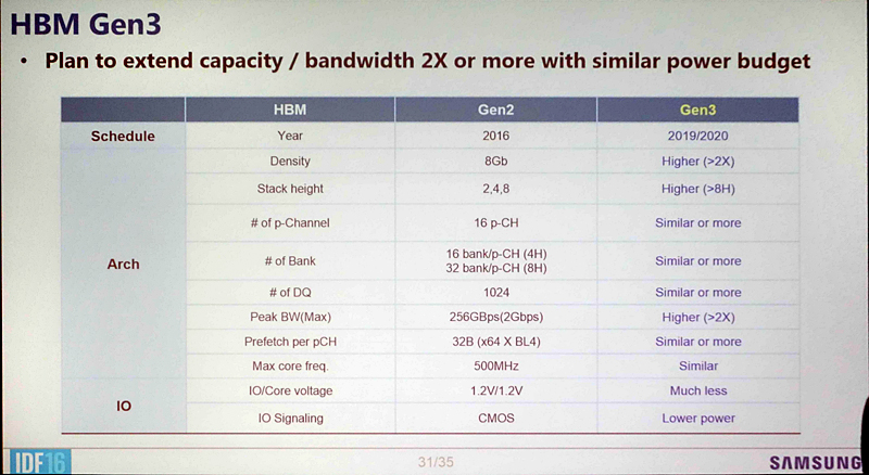
According to early HBM3 specs, HBM3 will exactly double both performance and density of HBM2, supporting up to 16GB per package (64GB total capacity) and up to 512GB/s of bandwidth per package (2,048GB/s total bandwidth). Core voltage is also expected to drop significantly as well which should lead to a decent reduction in power consumption.
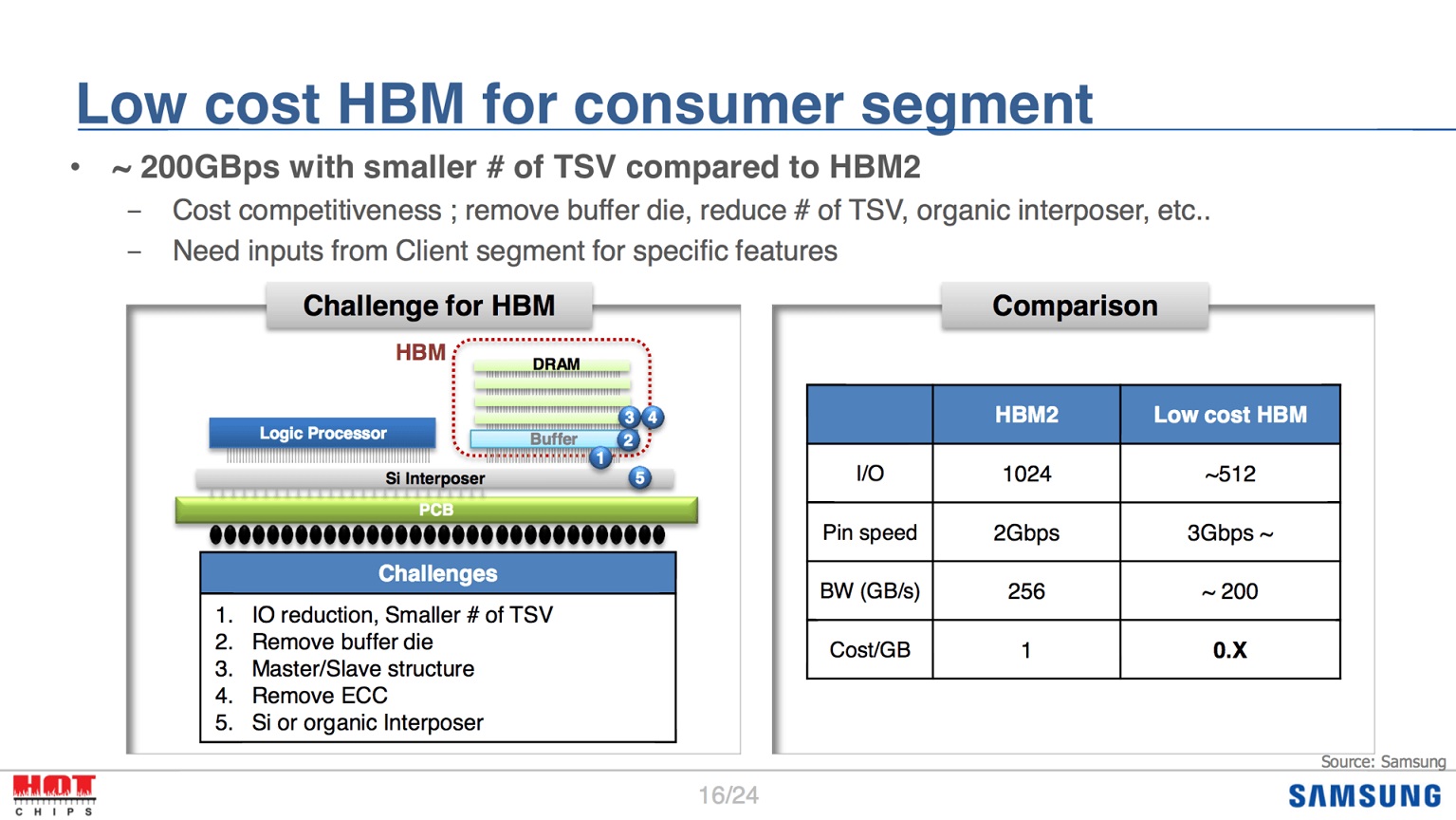
One issue with current generation HBM and HBM2 is its cost is generally prohibitive for implementation in consumer applications. Next generation HBM will attempt to address this with several power efficiency improvements including reducing the number of TSVs used, removing the buffer die, implementing an organic interposer, and more.
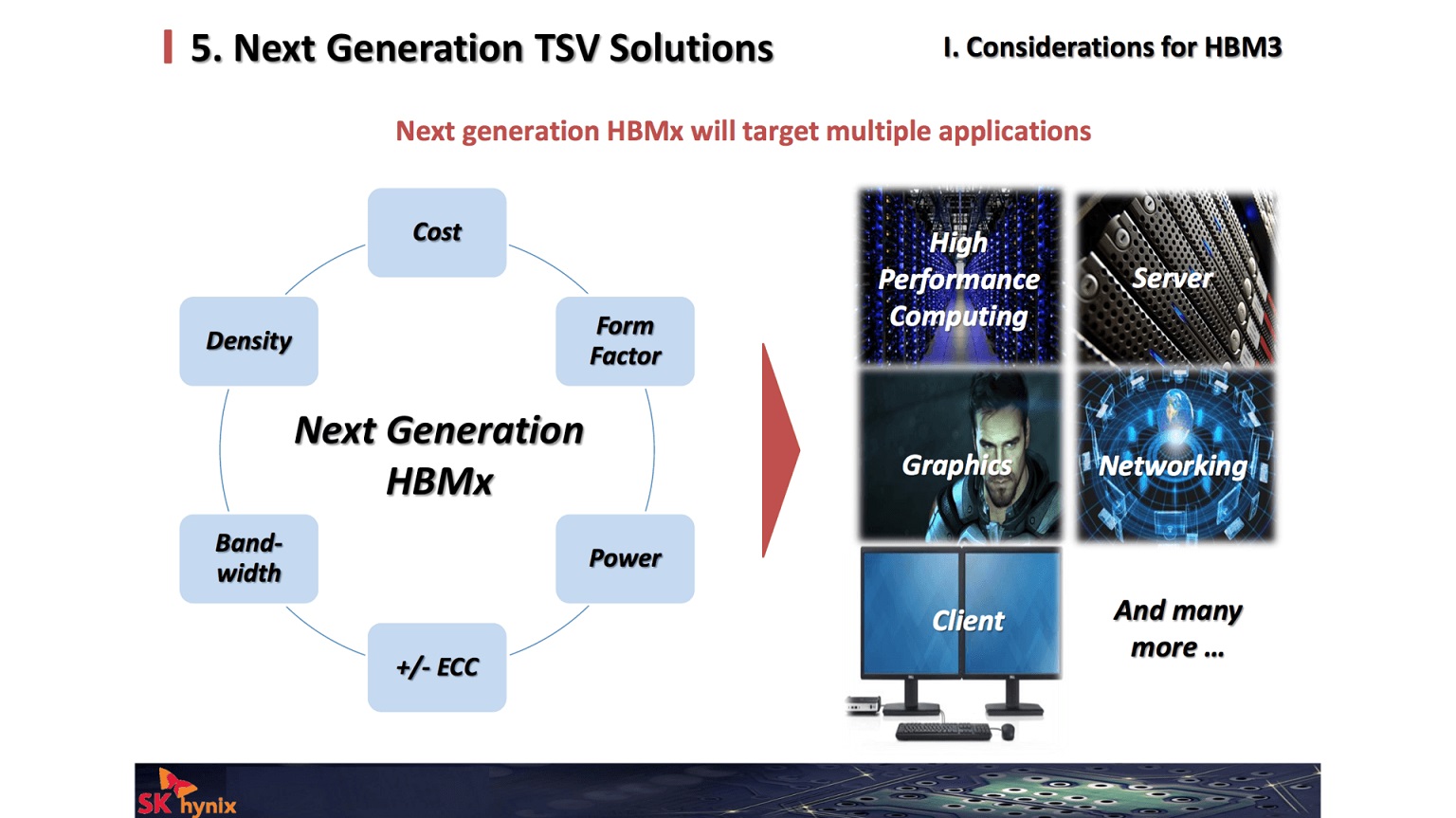
Next generation HBM is expected to initially target HPC applications, but trickle into server, graphics, networking and client applications down the road.
Source: ComputerBase, Videocardz


