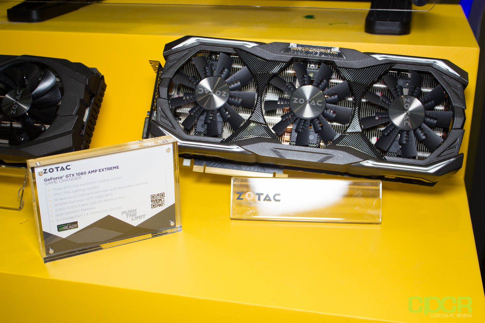
Well, we’re finally nearing the final launch of the Nvidia’s 28nm Kepler GK104 (allegedly also known as the GeForce GTX 670 Ti), so for those of you who can’t wait any longer, here’s some more pictures of the new GPU to help string you along until it actually comes out.

Here we’ve got a first look at the cooler itself with the shroud removed. It’s quite similar to what we’ve seen in previous generation GPUs, so it’s not much of a surprise here. You can also see that the card requires a pair of 6 pin PCIe power connectors, so it shouldn’t be a super power hungry GPU.

Next up, we’ve got an image of the front of the GPU. Here we spot some of the NVDD power phases along with some capacitors and some memory chips as well. Nothing too special here. The actual GPU itself was conveniently left out…. conveniently.

Here we’ve got the back of the PCB. We get to see some of the solder points as well as the GPU cooler mounting holes. It’s not too helpful though.

CENSORED! Yeah, that’s lame. We get a censored image of the new GTX 670 Ti, but it is proof that it exists and is in the hands of reviewers.

Yay! Uncensored! Just the way I like it. From here we can see the reference cooler design as well as the branding “GTX 670Ti”.
That’s all for today. I’ll update if anything else pops up. If you haven’t checked out the full length PCB leak, feel free to do so here. If you guys have something that I missed, drop it in the forums or the comments below!
Source 1: TechPowerUp
Source 2: TechPowerUp

