At the International Solid State Circuits Conference (ISSCC), AMD recently presented some additional in-depth information about the upcoming Zen micro-architecture used in their highly anticipated Ryzen CPUs.
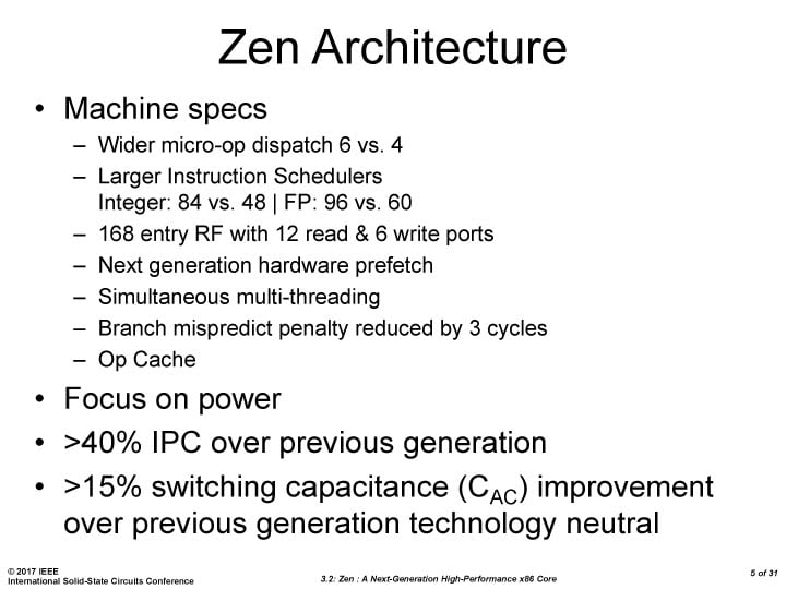
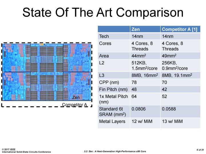
The AMD Zen micro-architecture is a complete redesign from the ground up and is the first AMD processor to utilize GlobalFoundries 14 FinFET process. It’s a 4 core design which is bumped up to 8 threads with AMD’s new SMT technology which allows a single core to process up to two threads simultaneously. It’ll also feature 32KB L1 cache per core, 512KB L2 cache per core and 8MB shared L3 cache. Interestingly enough, AMD Zen has double the L2 cache per core compared to “Competitor A”, aka Intel Skylake, despite the smaller die area of 44mm² (AMD Zen) vs 49mm² (Intel Skylake).
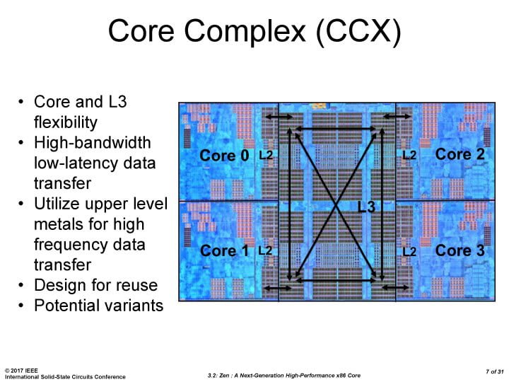
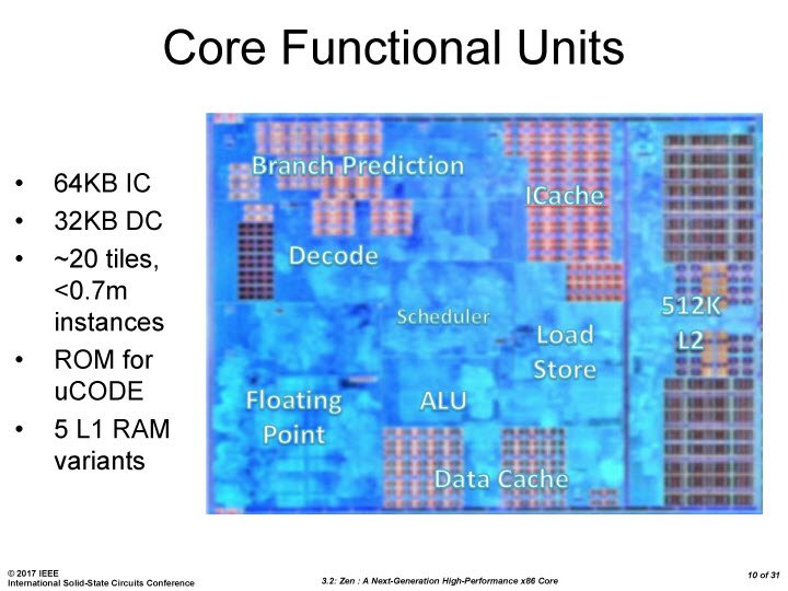
Here’s a look at the CCX as well as a in-depth image of the Zen core. Each core will feature four decoders with a ten pipeline design. The ten pipelines will include four ALUs (Arithmetic Logic Units), two AGUs (Address Generation Units), and four FP (Floating Point).
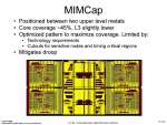
AMD has also significantly redesigned the cache architecture with the most significant being a move from using a write-through cache to a write-back cache. As such, this has significantly improved latency and performance as cache writes are confirmed immediately as soon as it’s written to the cache. This is the case for the L1 cache, L2 cache and L3 cache.
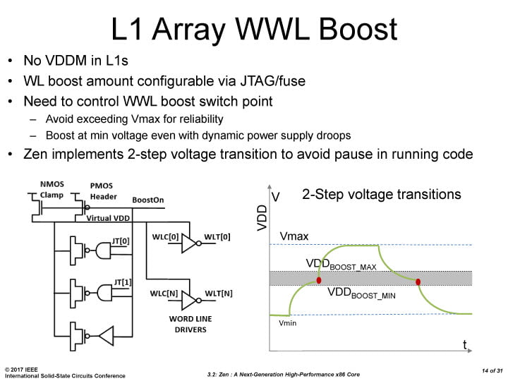
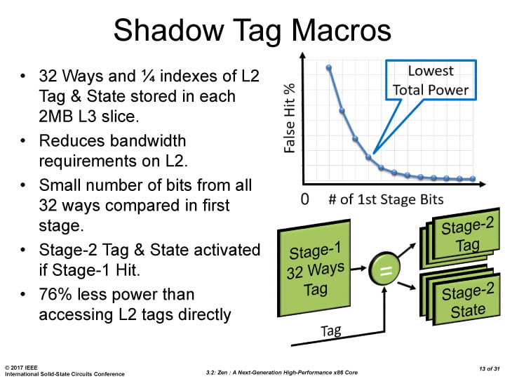
AMD has also improved power consumption of the cache by using new cache tagging technology which puts L2 cache data into the L3 cache reducing the need to go through the L2 cache. They’ve also introduced a new word line boost technology in the L1 cache reducing the minimum voltage needed for operation.
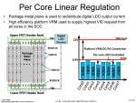
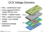
One of the biggest features of AMD’s Zen cores is the inclusion of a new digital LDO (Low-Drop Out) voltage regulator which is able to adjust voltages in real time based on the amount of load on each individual core in the CPU. As a result, the Zen cores are significantly more power efficient compared to the previous generation Bulldozer architecture.
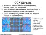
With Zen, AMD has implemented quite a bit of sensors including 1300 critical path monitors, 48 on-die high speed power supply monitors, 20 thermal diodes and 9 high speed droop detectors. These new sensors are a primary reason as to why AMD is able to offer XFR as the sensors are able to accurately detect temperatures as well as the minimum and maximum operating frequencies the CPU is capable of.
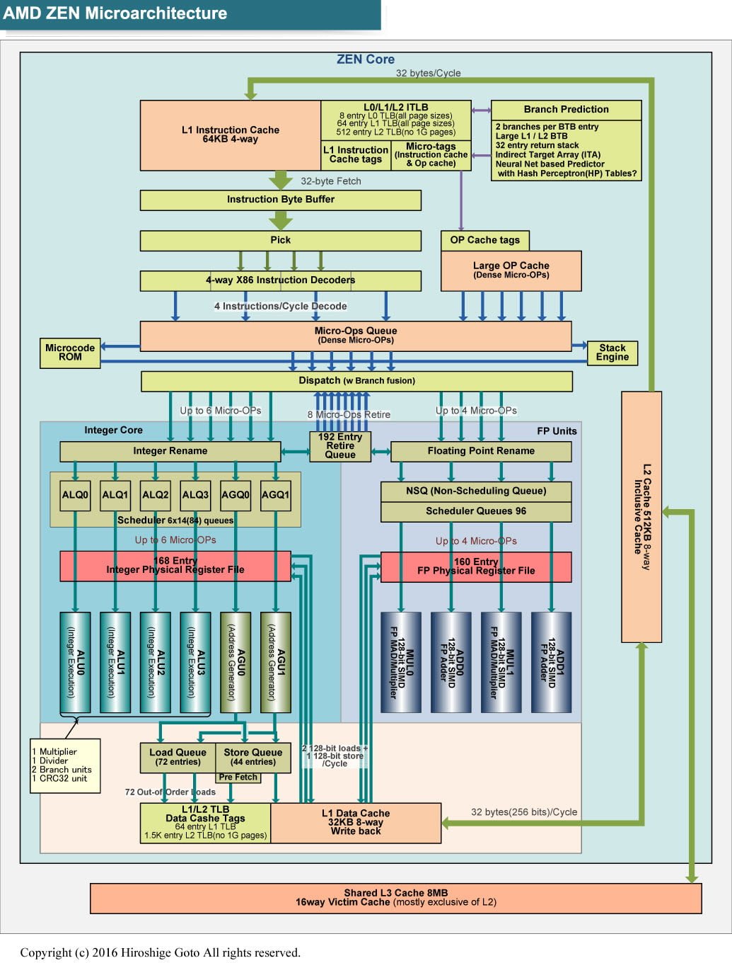
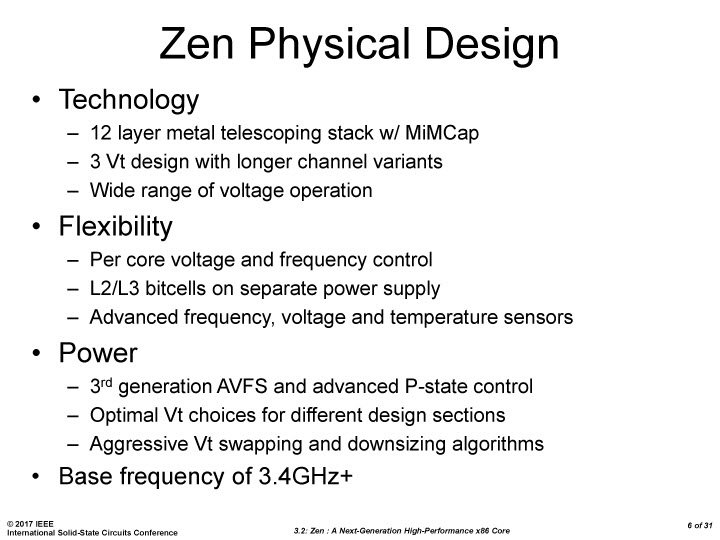
Here’s a schematic of the Zen core architecture.
In short, Zen is looking very impressive with some very solid technology behind it. The first AMD Zen architecture based CPU, Ryzen, is expected to begin shipping in early March.
Source: PCWatch
![The Best Black Friday 2017 Deals [Expired]](https://www.custompcreview.com/wp-content/uploads/2017/11/black-friday-image.jpg)