Several weeks ago, AMD made an announcement that their upcoming GPUs would feature a next generation memory technology called High Bandwidth Memory, or HBM. During the announcement very little information was shared about HBM, but AMD recently shared some more in-depth information on the technology.
The Limits of GDDR5
While most of you might’ve only heard of HBM for the first time a couple weeks ago, HBM isn’t really a brand new technology. It has been in the works for over 7 years now and was created through a collaboration of a number of companies, although primarily AMD and SK Hynix. The goal of HBM of course is to succeed GDDR5, which as AMD has pointed out has quite a few limitations.
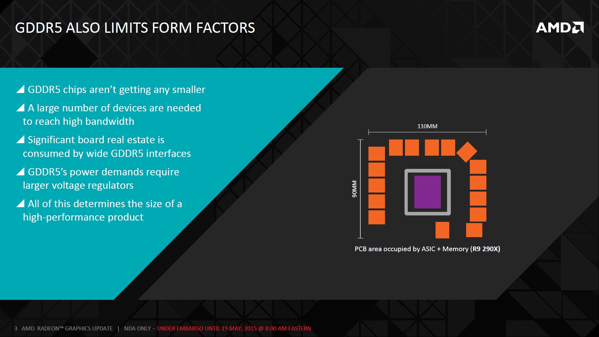
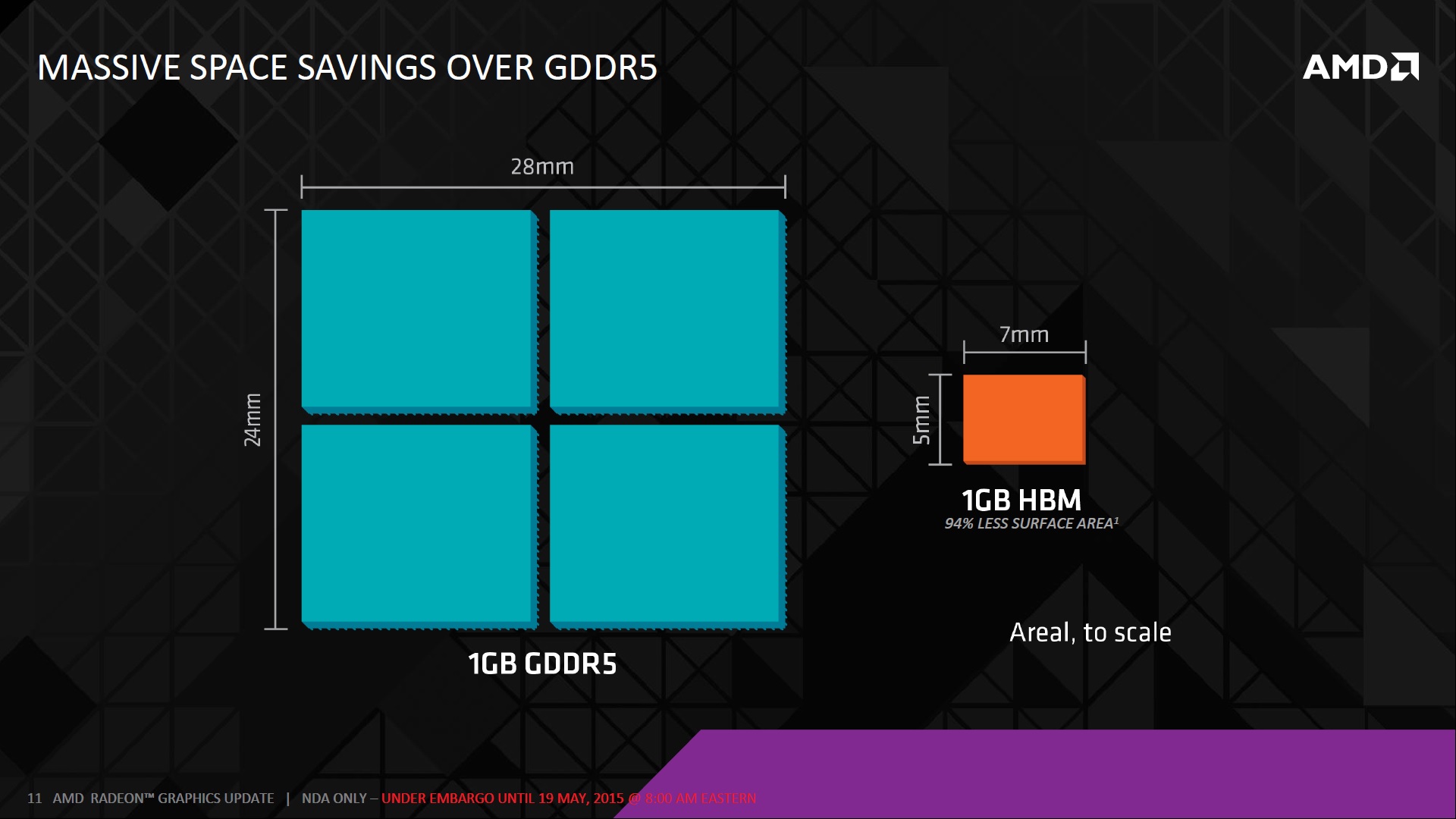
The biggest limitation with GDDR5 is that it requires a lot of PCB real estate. In order to get higher VRAM capacity and performance, a lot of GDDR5 chips are required. This of course requires a lot of space on the PCB, but additionally routing all these chips to the GPU has also become incredibly difficult as more and more chips are being packed into more and more advanced graphics cards.
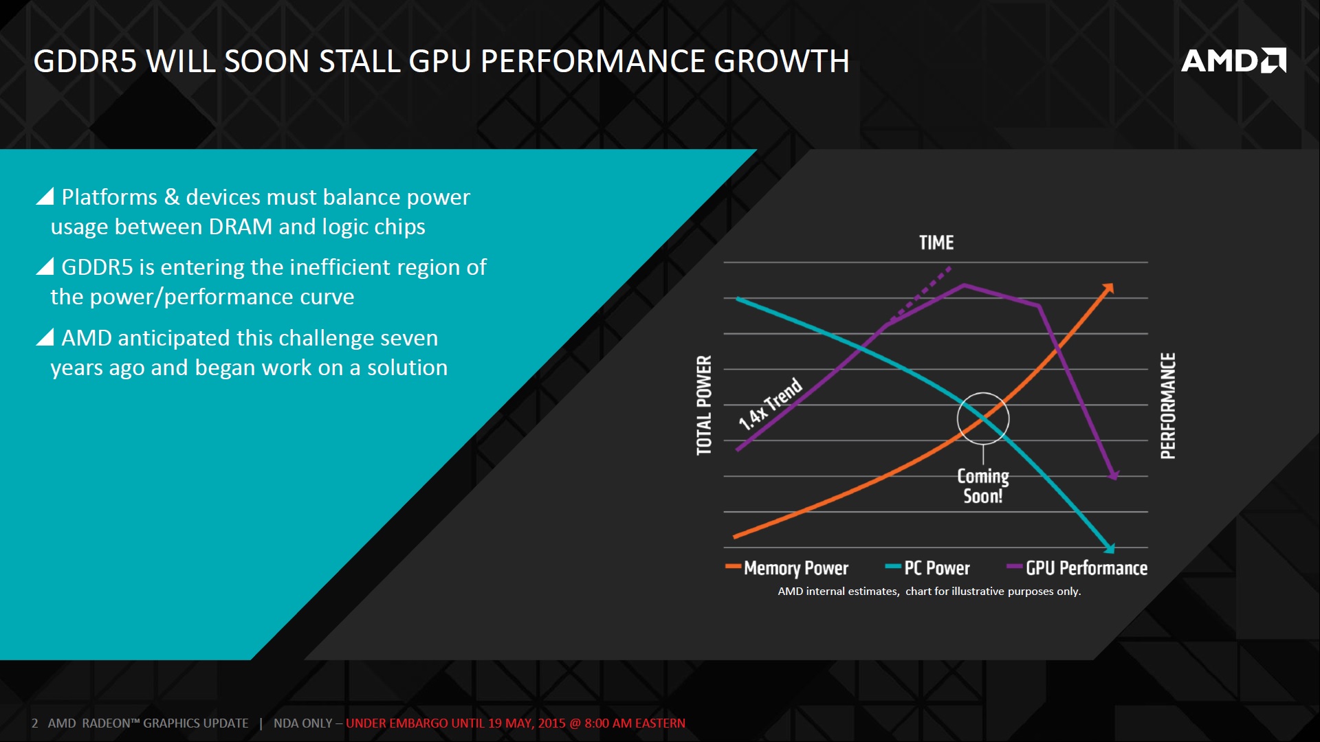
Another major limitation on GDDR5 is power to performance scaling. Just as we’ve seen on CPUs, GPUs, SoCs, etc. GDDR5’s power requirements skyrocket as clock speeds are continuously increased. This not only causes inefficiency with the GPU, but it also ties into the space limitation as additional voltage regulators become necessary.
Meet HBM (High Bandwidth Memory)
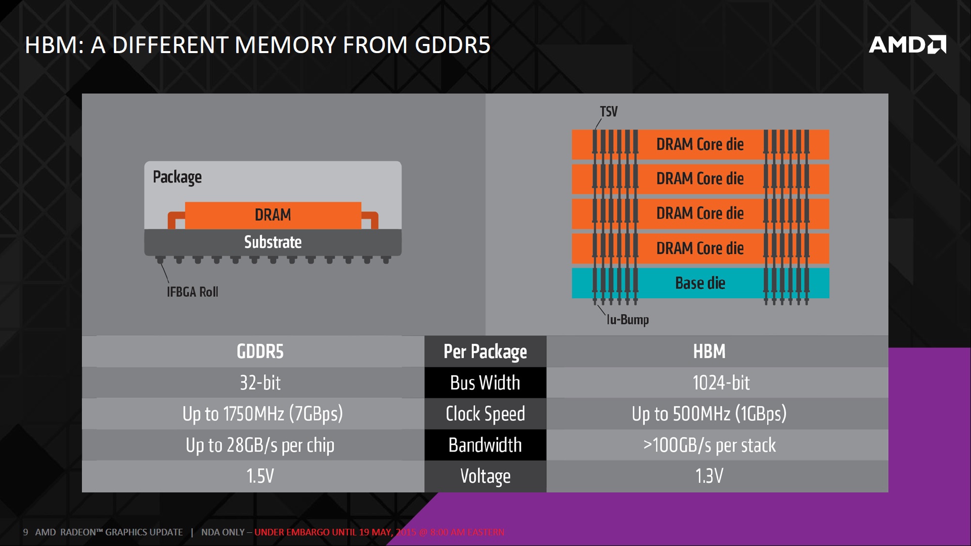
In order to tackle these problems, AMD needed to either change the way DRAM was designed or the way DRAM was packaged. In the case of HBM, AMD changed the way DRAM is packaged. As opposed to spreading many dies of planar DRAM around the GPU, HBM uses vertically stacked DRAM chips. Vertical stacked memory layers DRAMs dies on top of one another and communicates using Through-Silicon Vias, or TSVs.
All of the technical design translates into three main benefits – increased performance, lower power consumption, and reduced DRAM footprint. Each memory package on AMD’s first generation HBM implementation will contain a whopping 1024 I/O pins, a massive upgrade from GDDR5’s 8-32 I/O pins per package. Because there are more I/O pins per package, the bus width is significantly increased which allows HBM to run at lower clock speeds to produce higher performance than what’s possible with GDDR5. As high clock speeds are the primary driver of power consumption, HBM also operates at a lower 1.3V compared to GDDR5’s 1.5V. Additionally, since DRAM chips are stacked on top of each other, every package takes up significantly less space than an array of GDDR5 chips which means more room for other components or a more compact product.
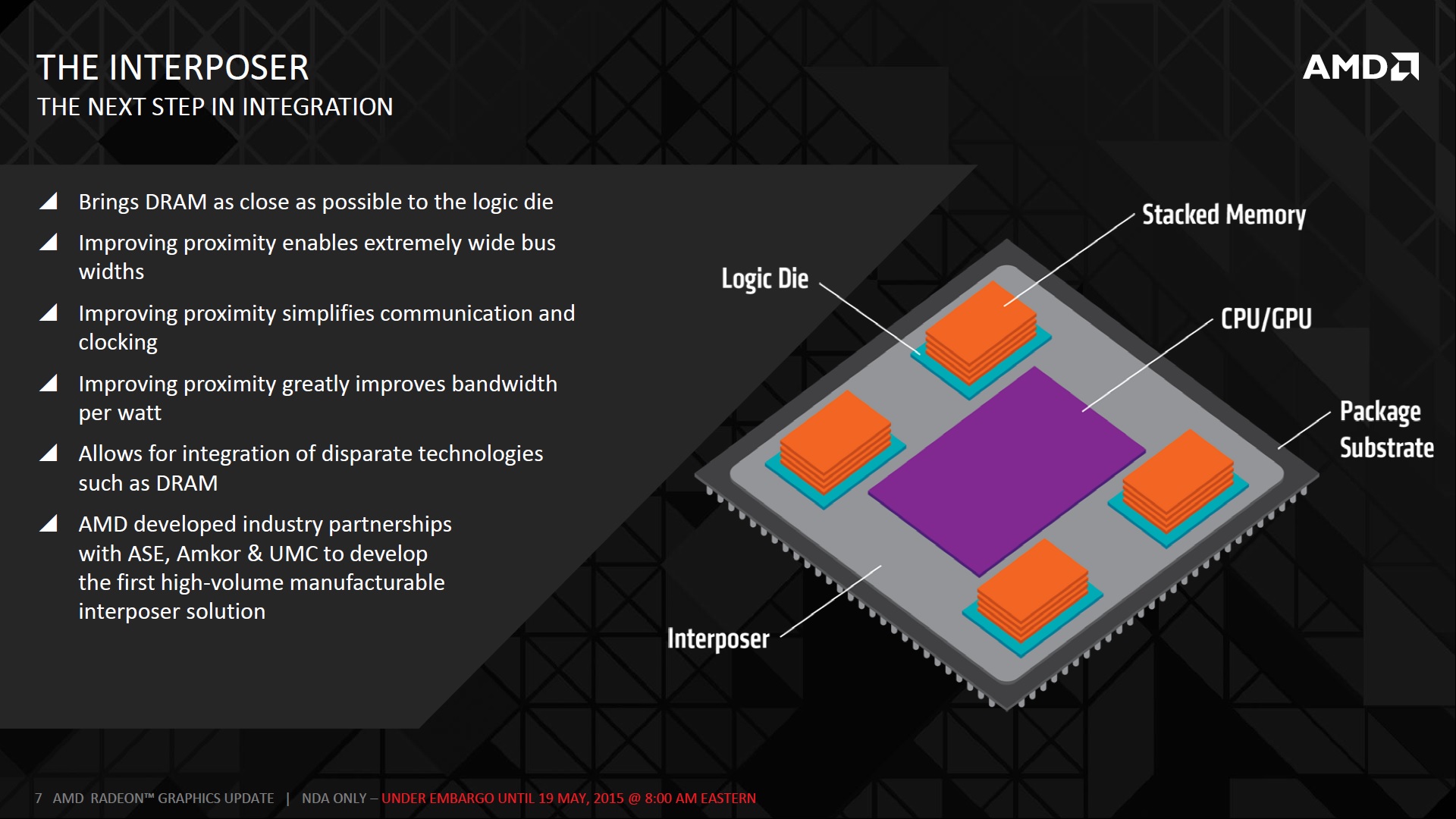
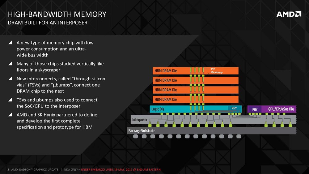
Since routing traces on the PCB was one of the big challenges with using GDDR5, AMD along with several partners also designed what they call an interposer, which sits between the GPU and the HBM DRAM. As seen from the illustration, the interposer brings the DRAM as close as possible to the GPU to further improve performance and power efficiency.
Final Thoughts
While HBM definitely sounds like the future of VRAM, it’s way too early to tell whether this will have significant tangible benefits in graphics performance. AMD hasn’t yet released any performance figures for their rumored Fiji graphics cards so we’re really left to guessing what an X percent increase in memory performance or X percent increase in energy efficiency actually means in frames per second or watts required.
That being said, Computex is rolling around soon and I’m sure we’ll be seeing more AMD in the near future. Stay tuned.
