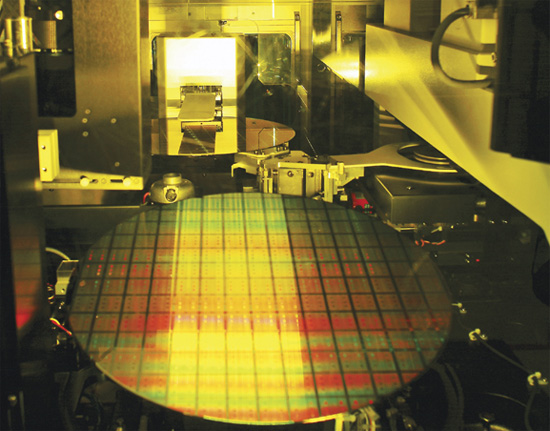
A new report from Electronic Times reveals that Samsung has recently completed development on 14nm planar NAND which is now in mass production. SK Hynix is expected to follow Samsung’s lead sometime in 2016.
While 2015 has been a banner year for Samsung’s 3D V-NAND, there’s still a huge market for cost effective planar NAND. A move from 16nm to 14nm represents a 12.5% reduction in size which has some major impacts on density and cost. By shrinking the die, this increases the amount of NAND that can be produced per wafer which in turn decreases production cost per die.
Previously it was expected that Samsung would abandon planar NAND development following the launch of their 3D V-NAND product; however, Samsung launched their 16nm NAND product earlier in the year and has further completed development on 14nm NAND as well. Planar NAND based on the 14nm manufacturing process is very tough to develop. With every manufacturing process shrink, the number of electrons that can be stored in a floating gate decreases. At the 14nm level, that could be just a few electronics per die, which seriously reduces the margin of error when reading or writing. This is the primary reason why most other memory makers have decided to cut development of planar NAND beyond 15nm.
Samsung has not yet stated whether or not it plans on development 3-bit MLC (TLC) NAND on the 14nm manufacturing process. Experts believe that they will face hurdles due to the same reason mentioned above. If successful however, production cost could be further reduced.
Source: Electronic Times

