[section label=1. Samsung Announces 256Gb 48-Layer 3-Bit MLC 3D V-NAND]
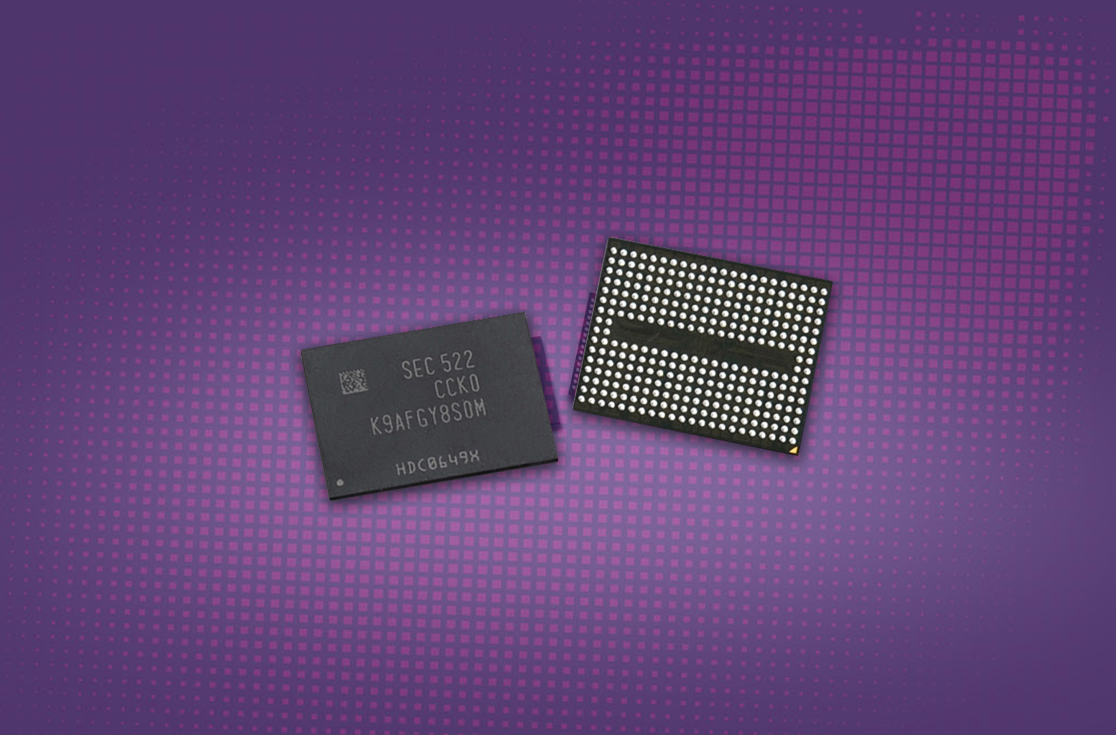
Samsung has begun mass production of the industry’s first 256Gb 48-layer 3-bit MLC (TLC)3D V-NAND flash memory just one year after the launch of their 32-Layer TLC 3D V-NAND.
The improved stack height allows for increased densities per NAND chip. The new 48-layer TLC 3D NAND extends the maximum storage-per-die ratio to 32GB/die, twice that of the current 16GB/die ceiling of 32-layer TLC. The higher density chips could easily be implemented to the current line-up of SSDs and double their capacities.
The new 3D V-NAND chips also cuts down on power draw and production cost. According to Samsung’s press release, Samsung’s 48-layer TLC 3D V-NAND reduces power consumption by over 30% compared to existing 32-layer TLC 3D V-NAND chips when storing the same amount of data. They could also be mass-produced with very little change to manufacturing equipment and has 40% increase in yield reliability.
Samsung plans to mass-produce its 3rd generation V-NAND from this point onward and focus on implementing them into its upcoming SSD products.
[section label=2. Press Release]
Samsung Electronics Begins Mass Producing
Industry First 256-Gigabit, 3D V-NAND Flash Memory
Stacks 48 layers of 3-bit-cell arrays to realize 32 gigabytes of data storage on a single chip with approximately 40 percent more productivity
SEOUL, Korea – August 11, 2015 – Samsung Electronics Co., Ltd., the world leader in advanced memory technology, today announced that it has begun mass producing the industry’s first 256-gigabit (Gb), three-dimensional (3D) Vertical NAND (V-NAND) flash memory based on 48 layers of 3-bit multi-level-cell (MLC) arrays for use in solid state drives (SSDs).
“With the introduction of our 3rd generation V-NAND flash memory to the global market, we can now provide the best advanced memory solutions, with even higher efficiency based on improved performance, power utilization and manufacturing productivity, thereby accelerating growth of the high-performance and the high-density SSD markets,” said Young-Hyun Jun, President of the Memory Business at Samsung Electronics. “By making full use of Samsung V-NAND’s excellent features, we will expand our premium-level business in the enterprise and data center market segments, as well as in the consumer market, while continuing to strengthen our strategic SSD focus.”
Samsung’s new 256Gb 3D V-NAND flash doubles the density of conventional 128Gb NAND flash chips. In addition to enabling 32 gigabytes (256 gigabits) of memory storage on a single die, the new chip will also easily double the capacity of Samsung’s existing SSD line-ups, and provide an ideal solution for multi-terabyte SSDs.
Samsung introduced its 2nd generation V-NAND (32-layer 3-bit MLC V-NAND) chips in August 2014, and launched its 3rd generation V-NAND (48-layer 3-bit MLC V-NAND) chips in just one year, in continuing to lead the 3D memory era.
In the new V-NAND chip, each cell utilizes the same 3D Charge Trap Flash (CTF) structure in which the cell arrays are stacked vertically to form a 48-storied mass that is electrically connected through some 1.8 billion channel holes punching through the arrays thanks to a special etching technology. In total, each chip contains over 85.3 billion cells. They each can store 3 bits of data, resulting 256 billion bits of data, in other words, 256Gb on a chip no larger than the tip of a finger.
A 48-layer 3-bit MLC 256Gb V-NAND flash chip delivers more than a 30 percent reduction in power compared to a 32-layer, 3-bit MLC, 128Gb V-NAND chip, when storing the same amount of data. During production, the new chip also achieves approximately 40 percent more productivity over its 32-layer predecessor, bringing much enhanced cost competitiveness to the SSD market, while mainly utilizing existing equipment.
Samsung plans to produce 3rd generation V-NAND throughout the remainder of 2015, to enable more accelerated adoption of terabyte-level SSDs. While now introducing SSDs with densities of two terabytes and above for consumers, Samsung also plans to increase its high-density SSD sales for the enterprise and data center storage markets with leading-edge PCIe NVMe and SAS interfaces.