48-Layer 3D V-NAND
When it comes to the NAND business, few companies can match the expertise of Samsung. Back in late 2013 Samsung introduced 24-layer 3D V-NAND, becoming the first NAND manufacturer to mass produce 3D NAND. Without skipping a beat, Samsung then introduced 32-layer 3D V-NAND in both 2-bit MLC and 3-bit MLC flavors a year later in 2014.
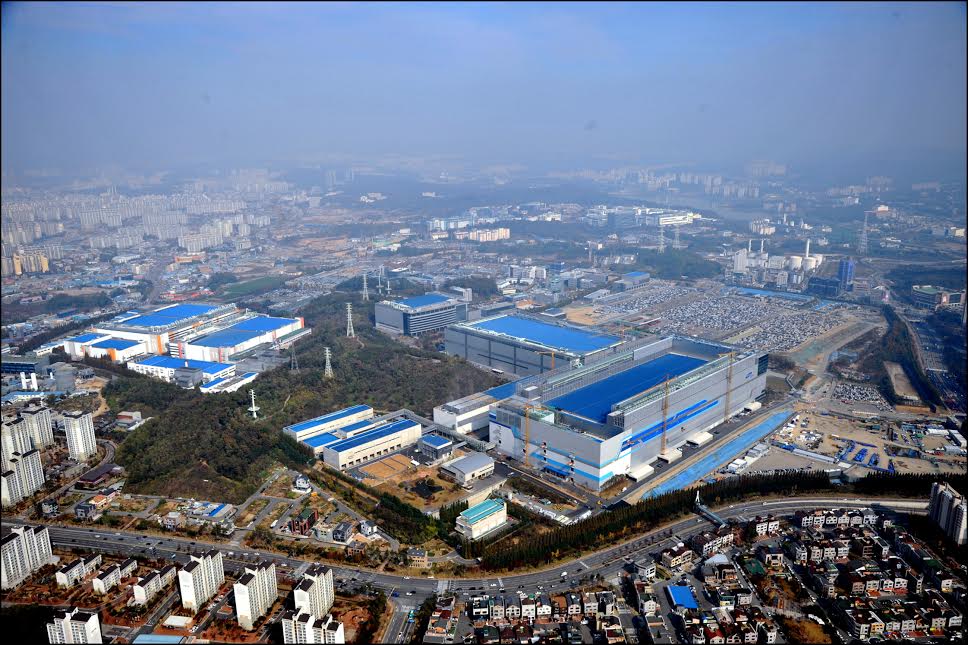
According to a new report by Korean IT site, ETnews, it looks like Samsung is preparing to begin mass producing 48-layer 3D V-NAND to continue to secure technological dominance against competitors SanDisk, Toshiba, Micron, and SK Hynix who are all expected to be launching 3D NAND products by the end of this year or early next year.
Furthermore, the report claims that Samsung is already seeing yields northwards of 80% on 48-layer 3D V-NAND and are making investments in their Xi’an facility to expand production from 50,000 units/month to 80,000 units/month. Additionally according to an unnamed source, 64-layer V-NAND is also in the works although no specific timeline on its expected release has been made available at this time.
Currently, 24-layer 3D V-NAND is being used in Samsung’s enterprise/datacenter SSDs and their 32-layer 3D V-NAND is being used in their consumer SSDs. It’s currently unknown whether 48-layer will be enterprise exclusive or will be used by both enterprise and consumer products. Samsung is expected to reach 256Gb die densities by the end of this year.
10nm Class DRAM
In addition to NAND, Samsung is also expected to develop a 10nm class DRAM, which is likely to be 18nm. According to industry rumors, Samsung is preparing to begin mass manufacturing of their 18nm DRAM product soon although no specific timeline is available at this time. Currently, Samsung’s most advanced DRAM manufacturing node is at 20nm.
10nm AP
The article also lightly touched on advancing to a 10nm AP (Applications Processor) node which is expected by the end of next year. Samsung recently began mass producing Exynos AP at the 14nm FinFET node.
Source: ETnews


