Although this week is Intel Developer Forum week, it hasn’t stopped AMD from stealing the thunder by unveiling a host of new details about their highly anticipated Zen CPU architecture.
Quantum Leap in Performance, Efficiency
Performance
As you’d expect, AMD has done quite a bit in terms of redesigning the entire CPU architecture with Zen when compared to previous CPU architectures to greatly improve performance.
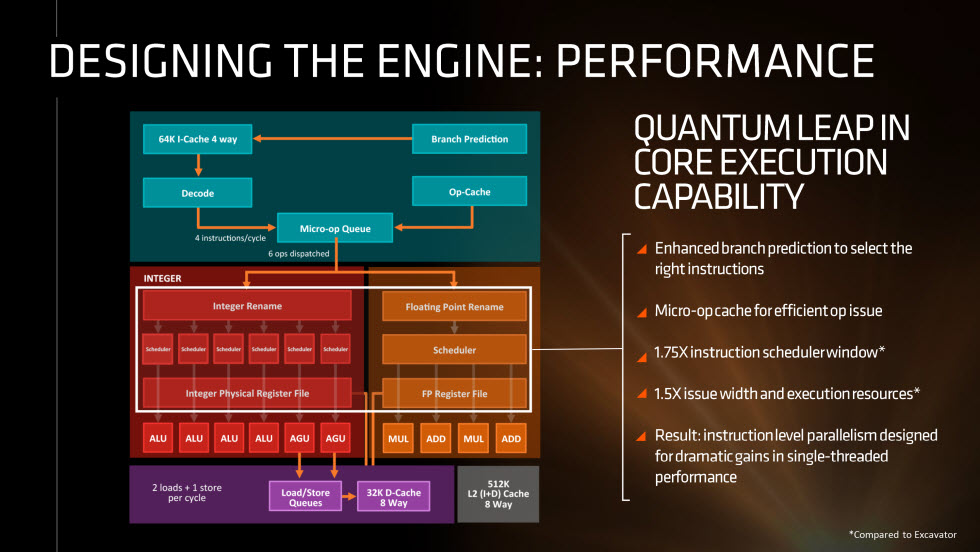
The biggest improvement here is likely going to be the micro-op cache. This allows the Zen cores to decode up to 4 instructions per cycle with an additional 2 thanks to the new micro-op cache. Previously, the Bulldozer architecture was only capable of decoding up to 4 instructions per cycle as it was missing the micro-op cache.
Zen also includes a 1.75x instruction scheduler window and 1.5x issue width which should significantly improve simultaneous processing.
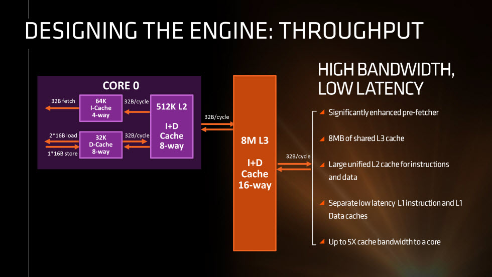
Looking a bit closer at the onboard caches, AMD has also made some massive changes here as well. The L1 cache is now separated between instruction and datastore with 64K going to the 4-way instruction cache and 32K going to an 8-way datastore cache. Below that an 512K 8-way L2 cache provides caching for both instructions and datastores and even below that, a 8M 16-way L3 shared cache provides caching for both instructions and datastores as well.
The biggest improvement here is that the L1 cache is no longer shared between two cores as in previous AMD architectures and the cache is now write back rather than write through for better performance.
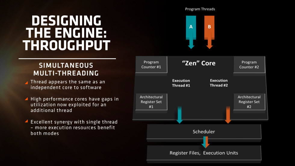
Further improving performance at the core will be simultaneous multi-threading which is similar to Intel’s Hyper-Threading. This will allow a single core to process multiple threads to improve core utilization on multi-threaded applications.
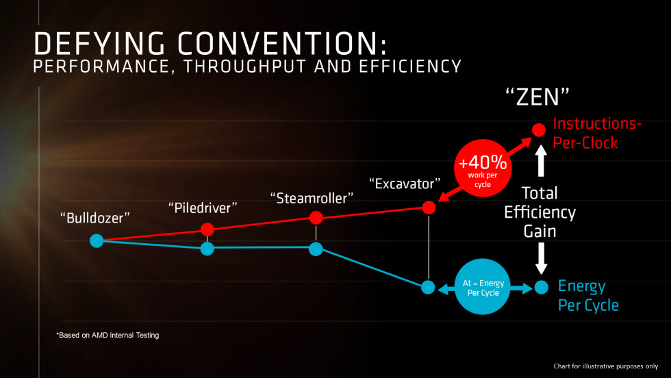
The combination of these performance and efficiency improvements is expected to result in a 40% improvement in IPC performance.
Efficiency
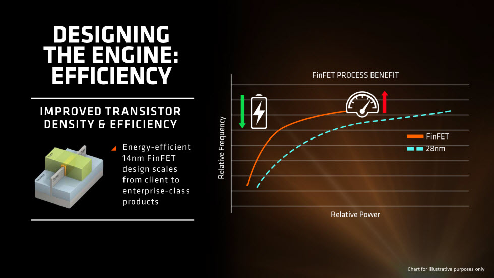
We’ve already seen the massive performance and efficiency benefits from 14nm FinFET from AMD’s Radeon RX 480 and the drop to 14nm FinFET should itself bring huge improvements in efficiency for Zen.
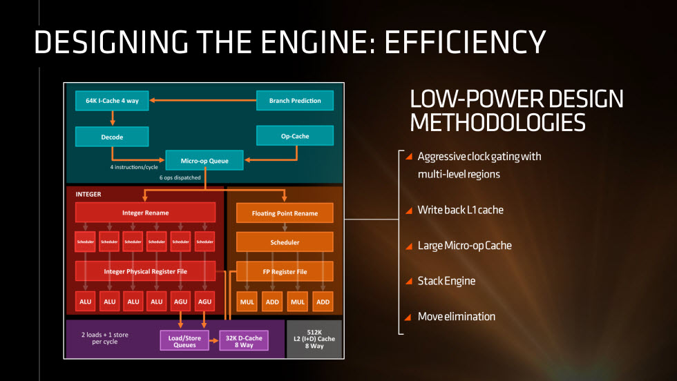
Further enhancing efficiency, Zen will be aggressively clock gated with multi-level regions so at any given point, so it will be very aggressive in attempting to shut down idle portions of the processor.
AMD is also implementing a write back L1 cache which was discussed previously. This will not only help power efficiency, but performance as well. Write back caches confirm completion of writes as soon as the write is written to the cache which is significantly faster than the write through cache seen in Bulldozer which require writes to be written through to permanent storage before being confirmed. In addition, the micro-op cache should further improve efficiency by caching certain frequently used instructions.
AMD has also implemented some other power saving features including stack engine and move elimination, both of which reduce the amount of processing needed for their specific operations.
Zen vs Broadwell-E Demo
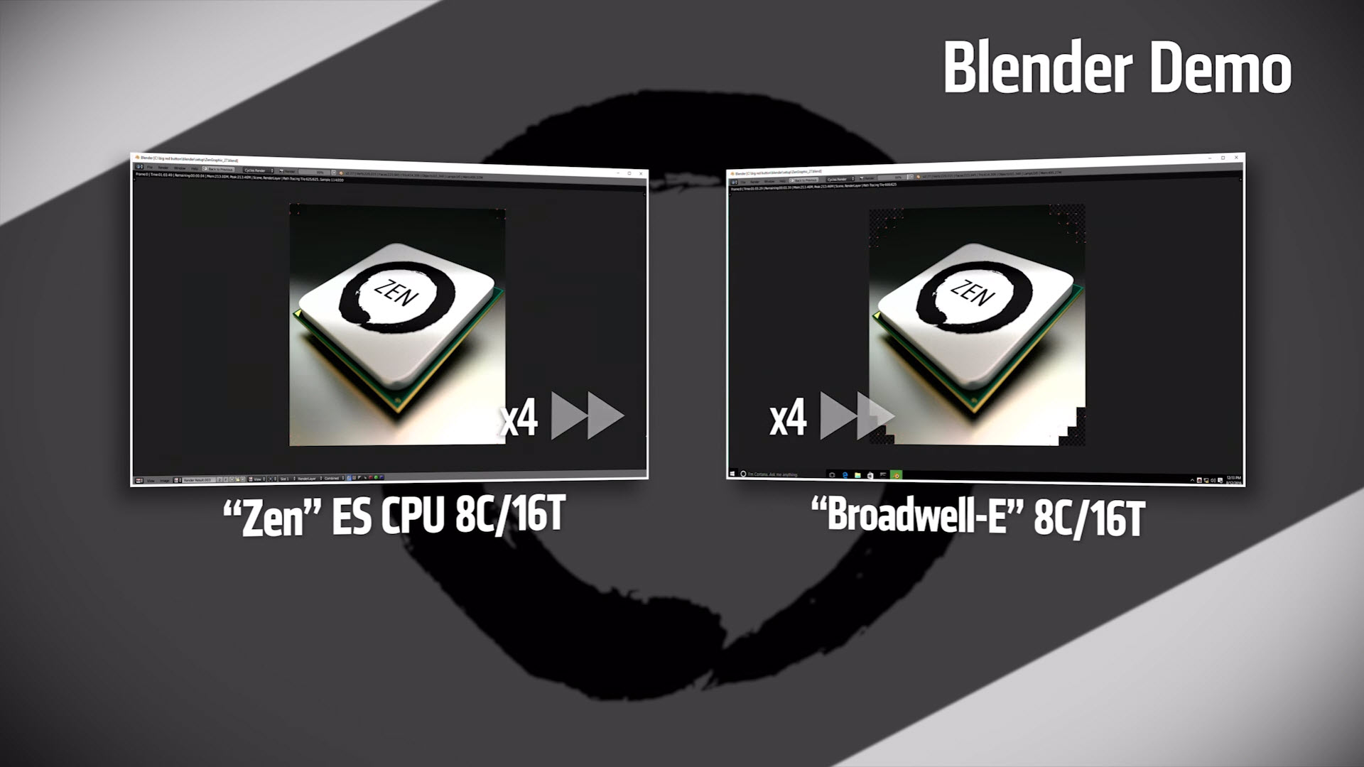
During the presentation, AMD also showed off a demo of an Intel Broadwell-E 8-core, 16-thread CPU vs an AMD Zen ES (Engineering Sample) 8-core, 16-thread processor both clocked at 3.0GHz for “Clock for Clock” testing. Here, the Zen ES chip was able to slightly beat out the Broadwell-E CPU which is one of the most powerful consumer CPU Intel makes.
AMD expects to begin shipping their new Zen architecture based CPUs in 2017 in the high end desktop market first with their 8-core, 16-thread CPU, codenamed Summit Ridge followed by a 32-core, 64-thread server CPU, codenamed Naples.
AMD is expected to release additional details on Zen’s underlying architecture as it gets closer to launch.
