[section label=1. Toshiba Announces Mass Production of 15nm NAND]
Once again, the SanDisk/Toshiba juggernaut takes the lead as Toshiba recently announced plans for mass production of 15nm 2-bit MLC at the SanDisk/Toshiba jointly owned Fab 5 in Yokkaichi, Japan. The new 15nm fabrication process will be the world’s finest 2-bit and 3-bit MLC NAND fabrication process with SK Hynix at 16nm, Samsung at 19nm, and IMFT trailing at 20nm.
In addition to the finer manufacturing process, Toshiba additionally claims that the new 15nm NAND will contain improved peripheral circuitry technology allowing the new chips to achieve the same write speed as 19nm NAND; however, with a new high speed interface will achieve a 533 Mb/s data transfer rate, a 1.3x improvement over 2nd generation 19nm NAND.
Toshiba is expected to begin ramping up production on 15nm 2-bit per cell 128Gb NAND beginning the end of the month followed by a ramp up on 15nm 3-bit per cell (TLC) NAND in June.
Source: Toshiba
[section label=2. Press Release]
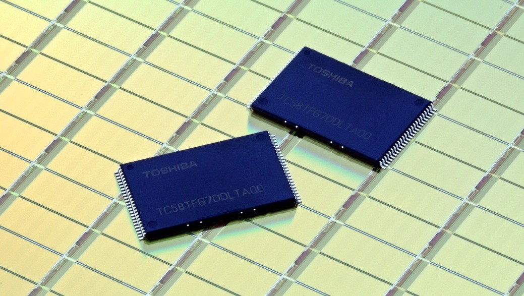
Toshiba Starts Mass Production of World’s First 15nm NAND Flash Memories
Toshiba Corporation (Tokyo: 6502) today announced that it has developed the world’s first*1 15-nanometer (nm)*2 process technology, which will apply to 2-bit-per-cell 128-gigabit (16 gigabytes) NAND flash memories. Mass production with the new technology will start at the end of April at Fab 5 Yokkaichi Operations, Toshiba’s NAND flash fabrication facility (fab), replacing second generation 19 nm process technology, Toshiba’s previous flagship process. The second stage of Fab 5 is currently under construction, and the new technology will also be deployed there.
Toshiba has achieved the world’s smallest class chip size with the 15nm process plus improved peripheral circuitry technology. The new chips achieve the same write speed as chips formed with second generation 19 nm process technology, but boost the data transfer rate to 533 megabits a second, 1.3 times faster, by employing a high speed interface.
Toshiba is now applying the 15nm process technology 3-bit-per-cell chips, and aims to start mass production in the first quarter of this fiscal year, to June 2014. The company will develop controllers for embedded NAND flash memory in parallel and introduce 3-bit-per-cell products for smartphones and tablets, and will subsequently extend application to notebook PCs by developing a controller compliant with solid state drives (SSD).
Toshiba continues to closely follow its process technology development roadmap and will strengthen product competitiveness and performance by applying leading-edge process to production. Looking to the future, Toshiba will reinforce its market leadership by promoting product innovation and development and ensuring that it is able to respond to a wide variety of clients’ product needs, including smartphones, tablets, slim notebook PCs and enterprise products requiring high reliability, including SSD for data centers.